
Homebrew ESD Safe Component Trays.
Assembling printed circuit boards is easy. You manufacture the PCB at location A, and then ship it to location B, along with some gerber files and a component list. The PCB is covered with a stencil that is used for applying solder paste. The PCB (with applied paste) is then fed into a pick and place machine that mounts the components, before it is fed into a reflow oven. Out comes your finished product.
In order to make it possible for pick and place machines to use a component in an assembly, the manufacturers will supply their components in either reels or trays. These go into a feeder mechanism that supplies the pick and place machine.
But what to do when you are producing small runs of modules that are supposed to be used as components in other assemblies ? An example of this is the EE02 LoRa module that is a component in the EE04 development kit. Hand soldering an EE04 board is possible (I know, since I have manually assembled eight of the prototypes), but one single board takes 2 hours to assemble manually. Production runs of 1-5 is manageable this way, but manually soldering a still relatively small run of 500 EE04 boards would take 1000 man hours, which would be prohibitive.
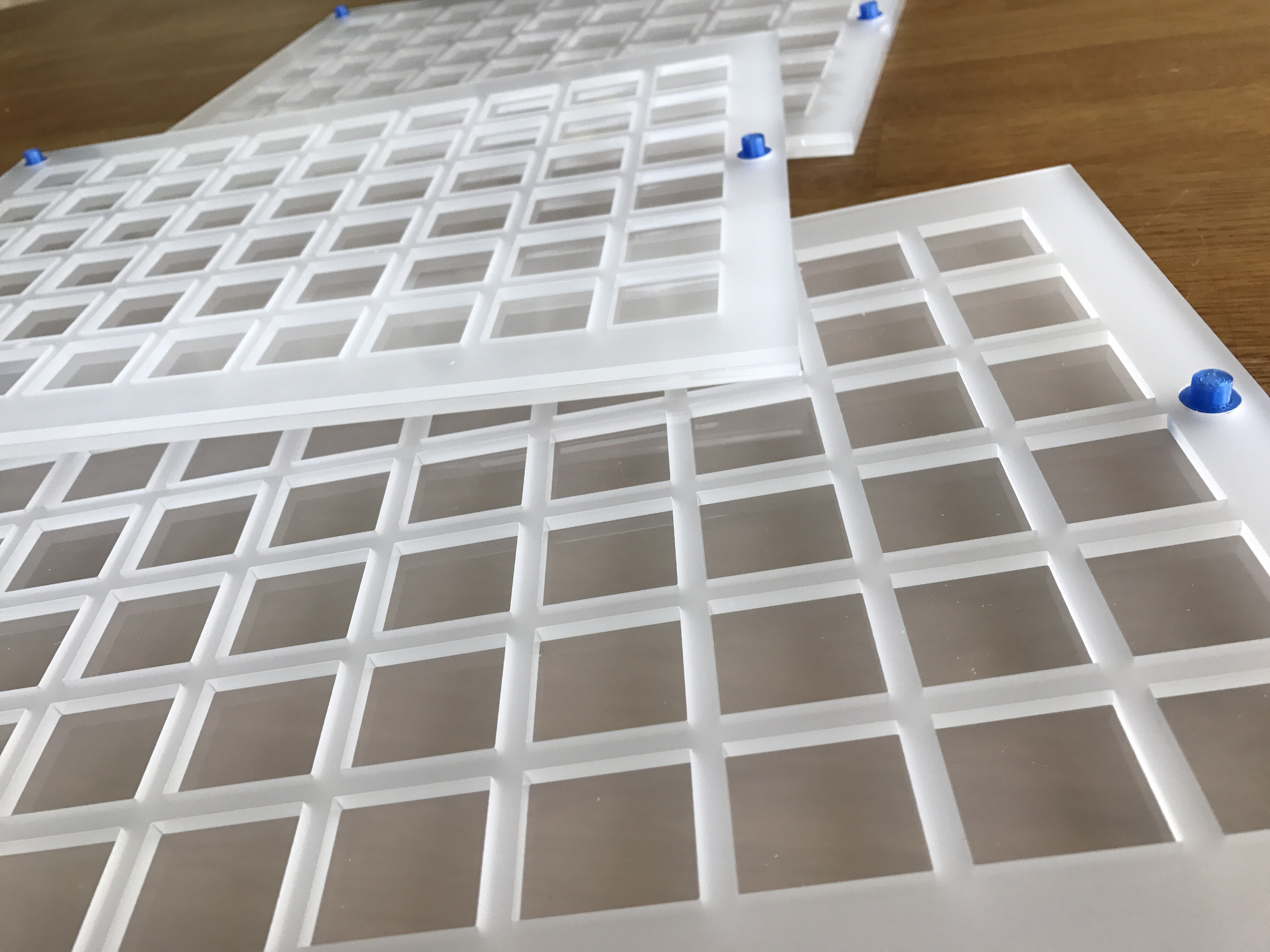
In order to facilitate automated assembly we were in dire need of component trays for our EE02 module. Such a tray would normally be injection molded from an ESD safe plastic. Creating a single injection mold requires CNC machining, which is expensive, and has to be outsourced to an external facility. Then using the mold would require another costly outsourcing step. In total, this approach would be prohibitively expensive for small runs. For our initial production run we will only need a few of the trays, but they are still mandatory for automated assembly.
So, what to do ?
We got in touch with Noca AS, wich is an electronics manufacturer here in Trondheim and asked for design constraints for component trays. We then applied these in order to create a CAD model of a tray that could hold our EE02s and also be compatible with their production line.
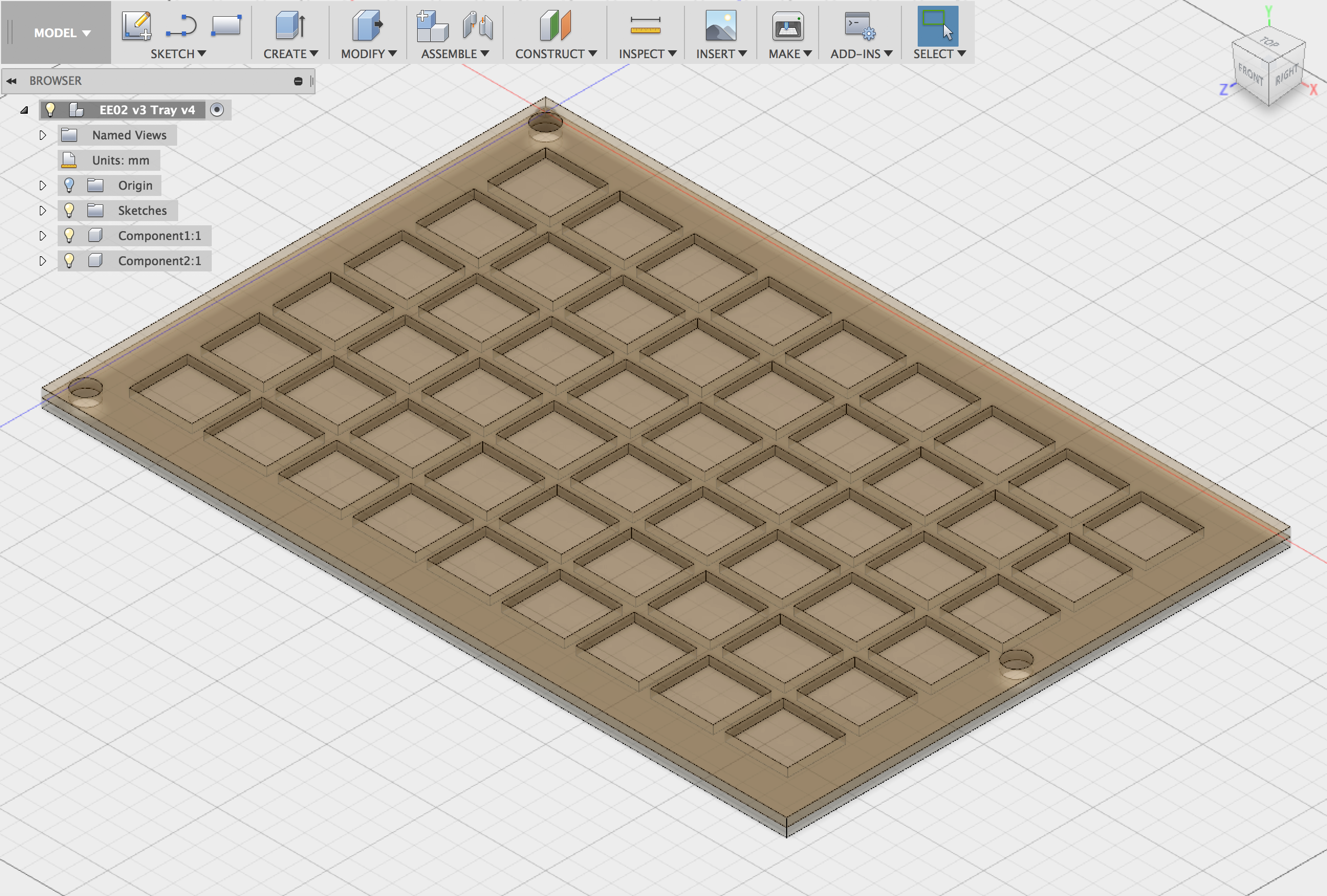
Such a model can be used for 3D printing, laser cutting or CNC milling. We initially attempted 3D printing, but we were not satisfied with the results. Printing large objects is a process that is error prone and also slow. Injection molding was not an option, so we decided to attempt laser cutting instead. The only problem being - that we didn’t have a laser cutter.
Hackheim makerspace
I got in touch with Hackheim (our local Hacker-/makerspace here in Trondheim). I have been a card carrying member for some time and knew that they had recently finished a fund raising campaign in order to be able to purchase a laser cutter from Full Spectrum Laser. Hackheim agreed to let us rent access to the laser at a very modest hourly rate. Big thanks to Hackheim !
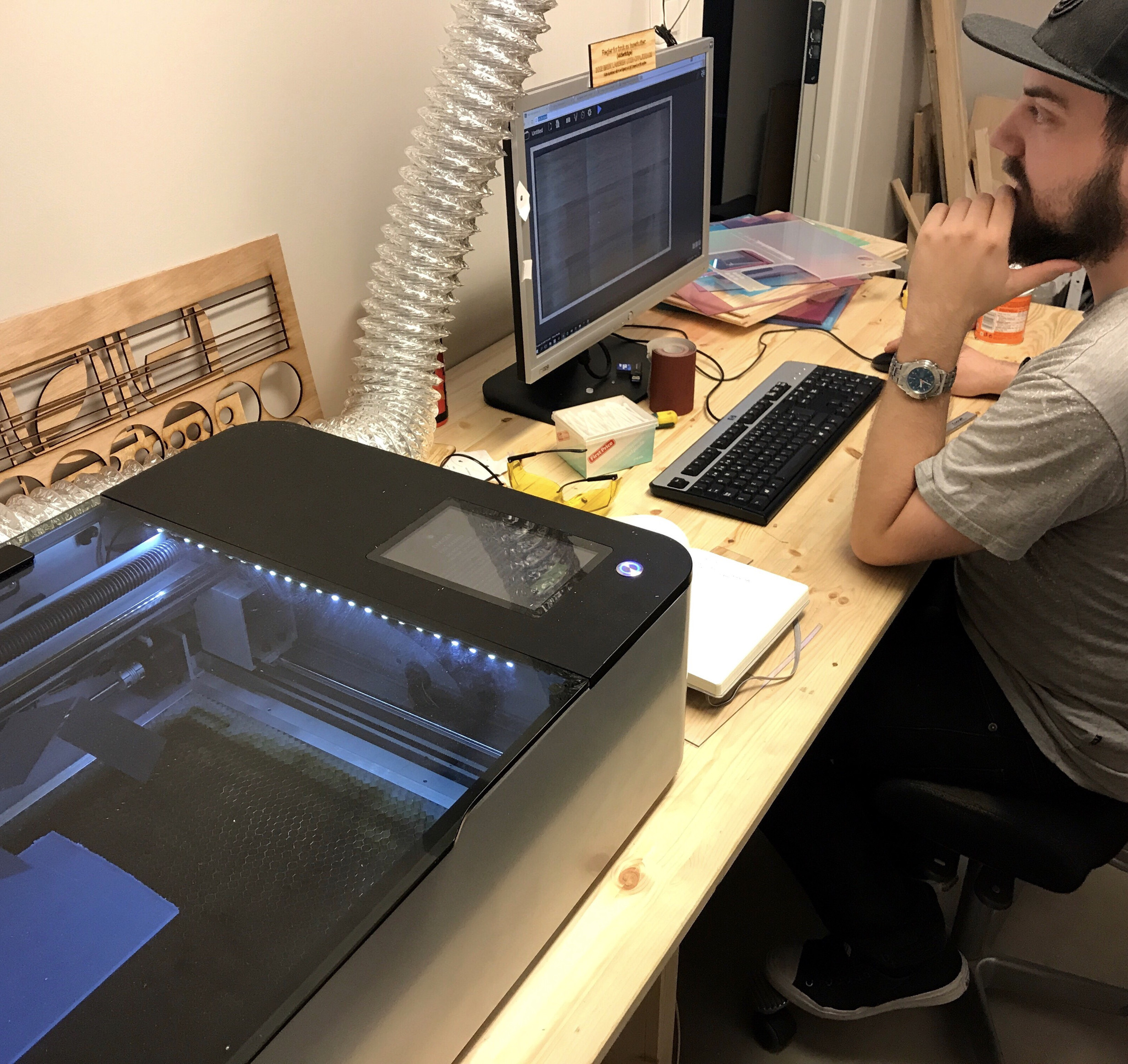
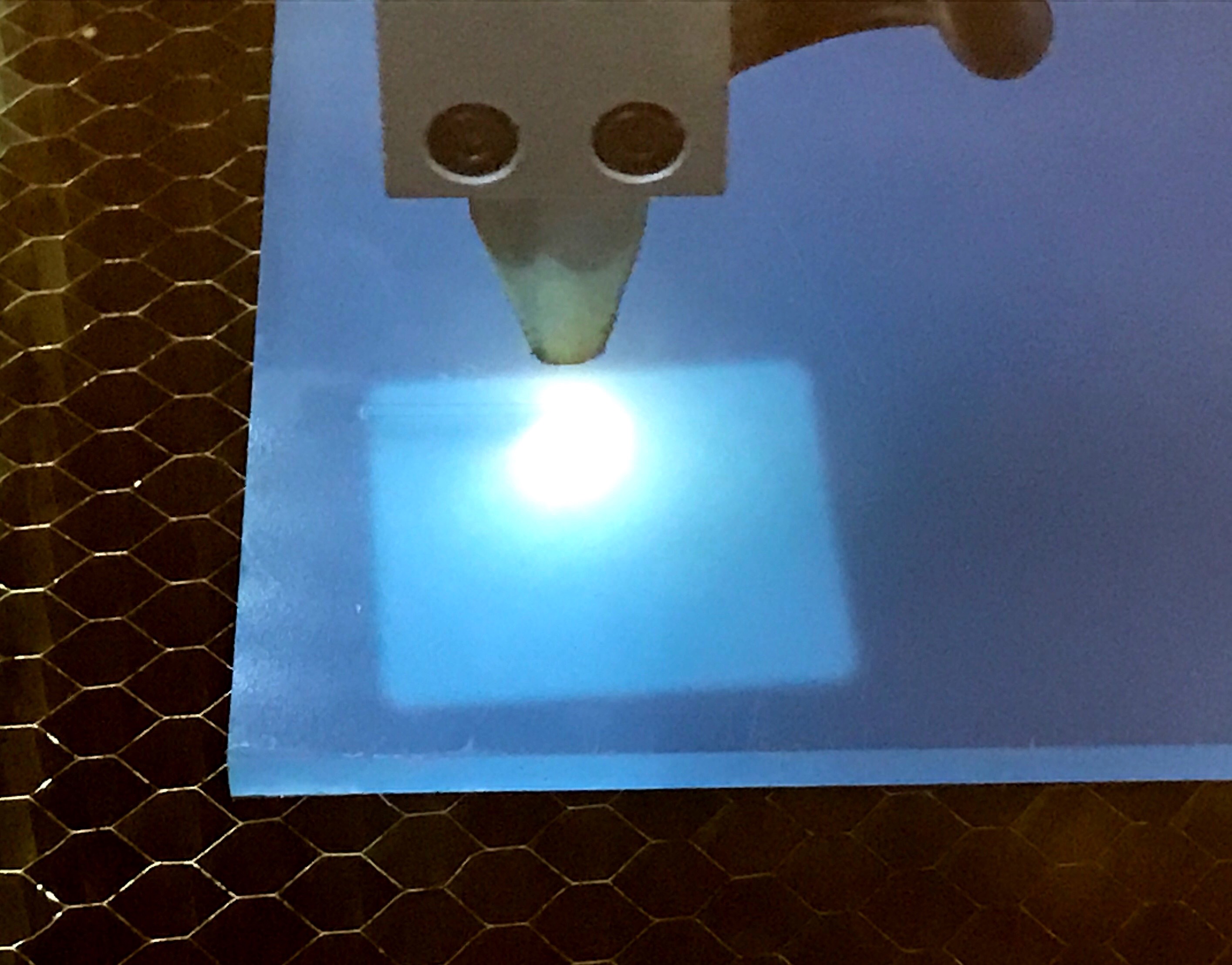
I then went on to purchase a stack of 4mm 600x600mm acrylic sheets and chopped them into laser friendly sized chunks, since the cutting area of the laser is limited to 500x300mm. The model surface sketches had to be exported as DXF from Fusion 360 and then converted into PDF before we could feed the designs into the laser (Clunky, but it still beats the Corel Draw frontend you can expect from Chinese lasers).
The trays are constructed by laminating two 4mm thick sheets of acrylic.
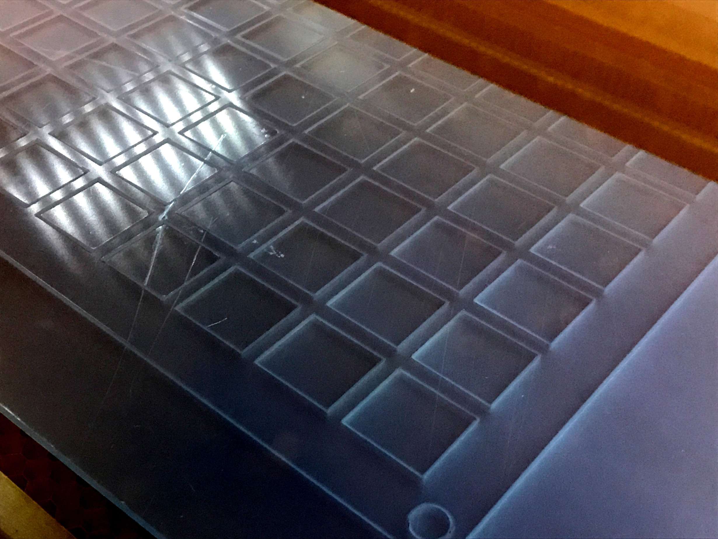
The laser cut the six necessary sheets for assembling three trays in approximately 90 minutes. I 3D printed custom knobs that could be inserted in the acrylic sheets, in order to make these stackable at the factory. The acrylic sheets where then glued together by “painting” the edges with acetone. The acetone spread evenly between the sheets of acrylic by capillary effect. Acteone is strictly speaking not a glue, but a solvent that dissolves acrylic. This results in a very strong bond between the parts.
One problem remained.
The trays needed to be ESD safe and acrylic is not an ESD safe material. We needed more chemicals. Exotic ones. Yay !
We found a supplier of ESD coating that would adhere to a variety of plastics, including acrylic. I ordered two quarts of “Staticide” and applied two coats to each of the trays.
And then (after waiting a few days for the coating to set before shipping the trays to the manufacturer) - we were ready to go into production. Yay ! That is - we had to wait for an available time slot at the manufacturing facilities at Noca.
Factory Visit
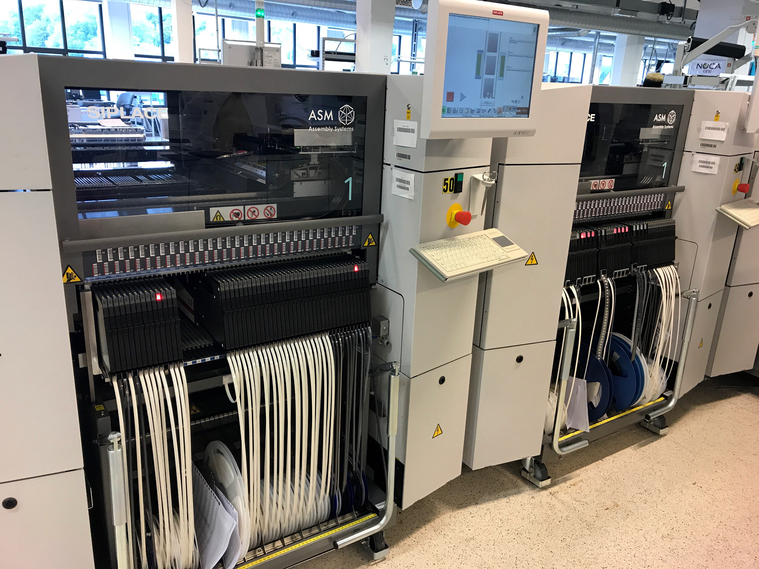
Noca called to inform us that they could fit us in for a pre production test run of a couple of panels. We packed our testing gear and jumped into a taxi, heading for the factory.
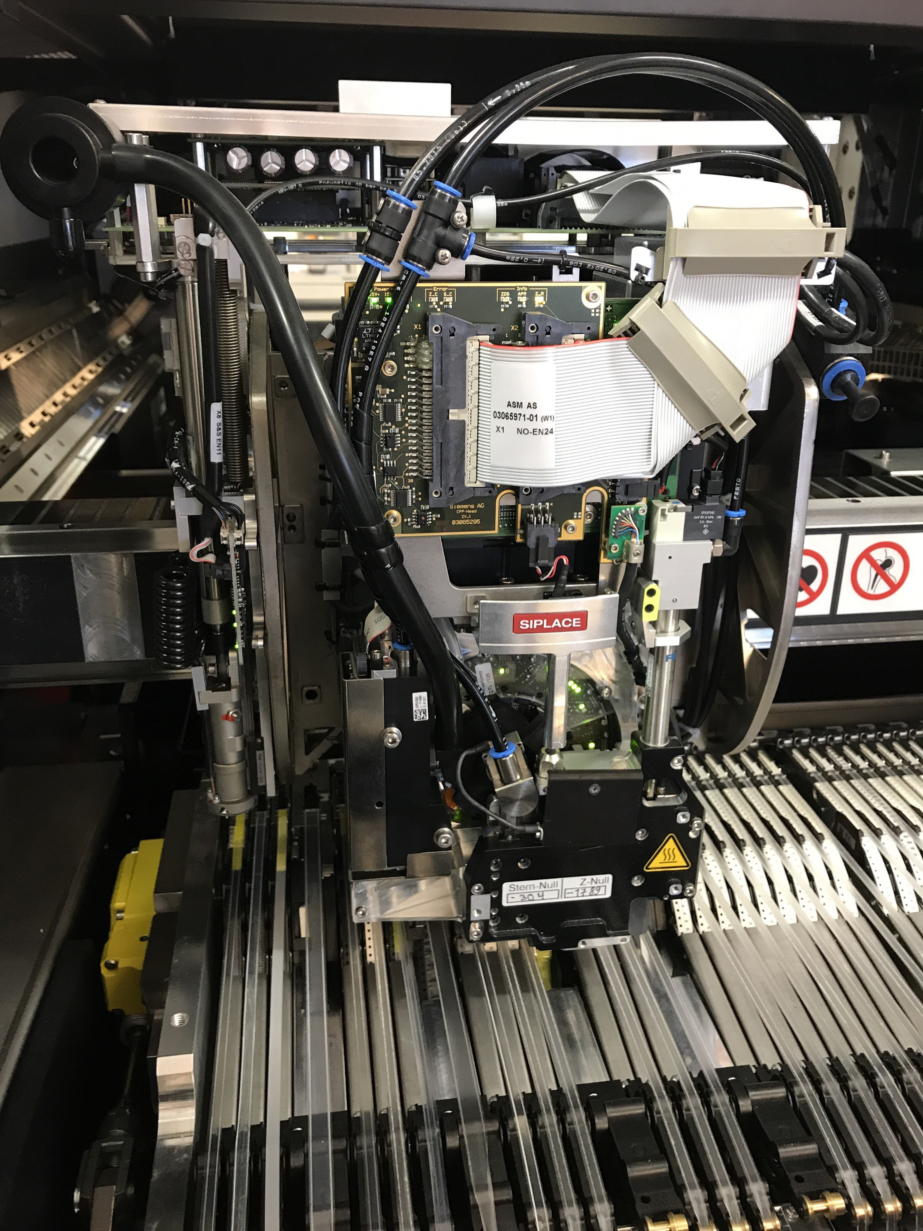
The production line was rather impressive. Peeking inside the machines was like poking your head into a mechanical candy store of the future. Gatlin gun style rotating vacuum heads or magnetic linear actuators, anyone ? :)
The Process
(…in which our trays take part. Just sayin’ :))
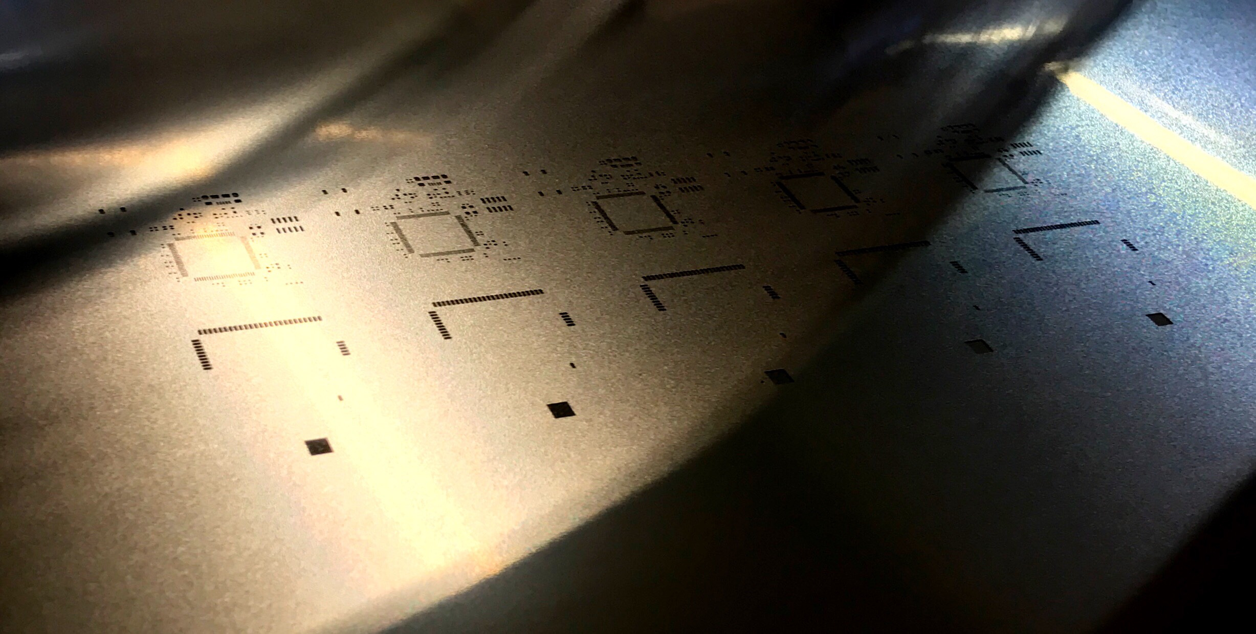
Step 1 - Solder paste
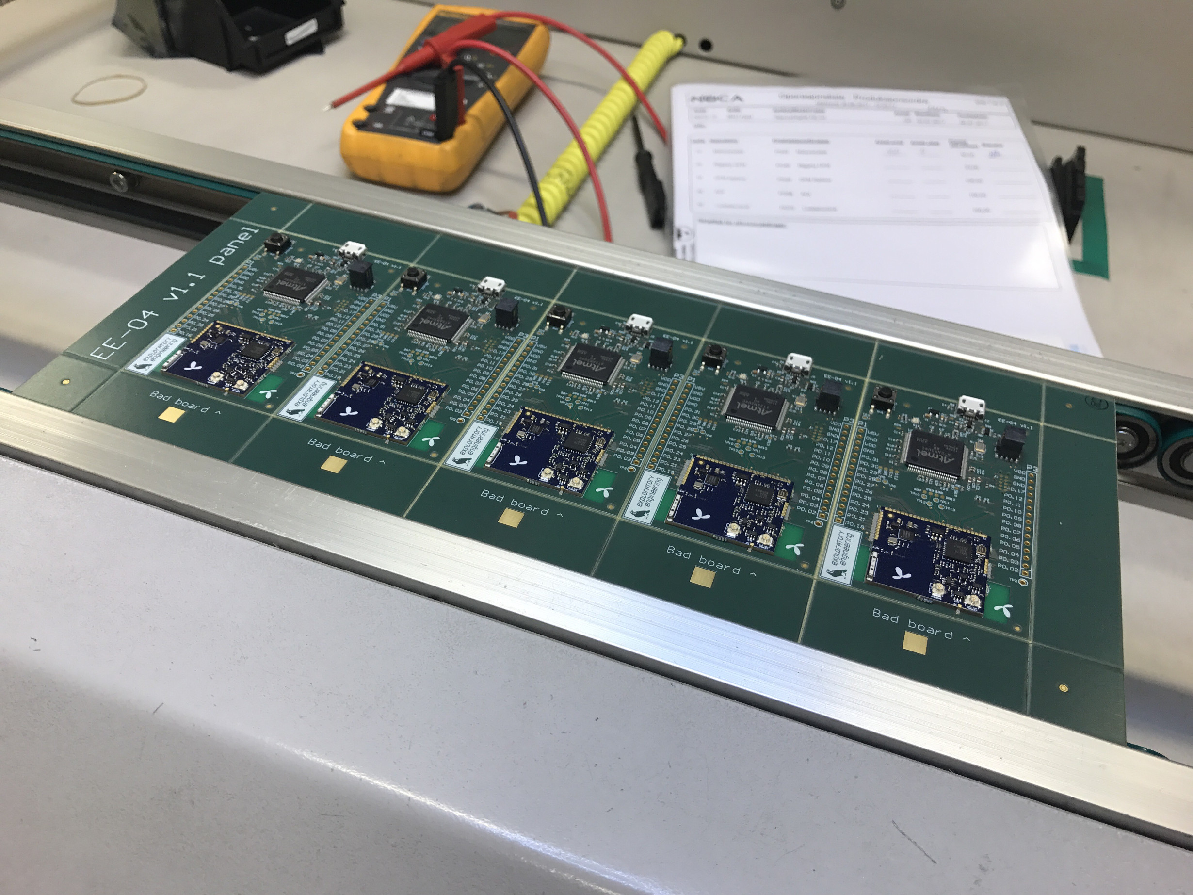
Solder paste is first applied to the PCB, using a stencil from the PCB manufacturer. The layout has 5 EE04 PCBs in a single panel. After pste application, the boards are automatically fed into the next machine.
Step 2 - Components.
Components are loaded into feeder mechanisms, that in turn are loaded into the pick and place machine. The Pick and place machine has several vacuum heads that pick components from the feeders and then orients and positions them in the correct location on the PCB. Watching the operation of these machine is an impressive sight. High speed machines can place 50000 components pr hour, which easily beats human assembly/soldering speed by four orders of magnitude.
 Above: Two P&P machines loaded with feeders, containing components for our EE04 development kits.
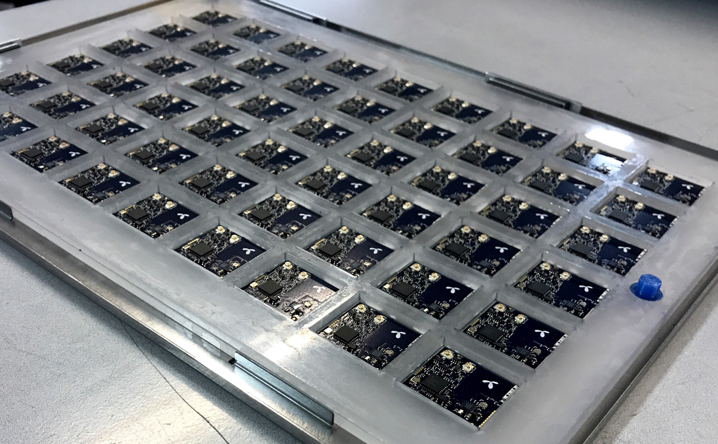 Above: Our homebrew EE02 tray before being inserted into the pick and place machine at Noca.
Step 3 - Manual Inspection.
There is always room for error. Manual inspection before soldering is done in the pre production run, in order to ensure correct component orientation on the PCB.
Step 4 - Reflow Soldering.
This is rather boring to watch, since it happens inside a reflow oven. Soldering all the components takes approximately five minutes - and afterwards a finished panel appears at the end of the production line.
Step 5 - QA - the boring part.
Like I said - there is always room for error. This is the part where we find out if there are any bugs in the design. We picked a few boards from the pre production run and executed the following steps.
- Flash the SAM bootloader. This SAM chip acts as a programmer for the EE02.
- Load the SAM chip with our custom Segger image. This firmware makes it easy to debug and deploy new firmware on the EE02 target module. When you connect the EE04 to your computer via USB, the programmer will be mounted as an external disk. A compiled image for the EE02 can then be dropped on the JLINK disk and the SAM chip will take care of flashing the EE02.
- Build a “Hello World” program and deploy it on the EE04. Connect with JLINK and verify that it runs on the EE02 (while taking note of the NRF52’s logged serial number).
- Connect an external EE02 to the EE04 and deploy the same image. Connect with JLINK and verify that it runs - this time with a different serial number.
All tests passed with flying colours. Say hello to the worlds first official development kit for the EE02 LoRa module - the EE04! Yay!
