I set out to familiarize myself with the BG95-M3 LPWA module from Quectel this winter. If you are a software developer (like me), transitioning to doing simple digital hardware prototypes is easier than you might think. A bit is a bit and it really doesn’t matter if it is represented as a digit or as a voltage level. Bits are easy :)
However, once you start moving into analog (and especially RF) territory, things tend to get more complex. At times, mind-bendingly so. Especially for those of us that don’t have degrees in electrical engineering and also know next to nothing about transmission lines and antenna theory. “Squishy” analog stuff is not for the faint hearted. More on that later.
Apart from the official BG95-M3 development kit from Quectel, I haven’t seen too many alternatives that lend themselves to easy prototyping with this module. The only possible exception is a BG95 PCI Express PCB module, that is available from AliExpress.
I decided to attempt to design my own breakout that could be used as an IoT connectivity module in application prototypes. What better way to get to grips with new hardware ?
I first had to decide on which CAD tool to use. I considered doing the schematics and board layout in Altium Designer, since Altium has features that help keeping stuff impedance matched. However, since the breakout most likely will be open sourced, it made more sense to do the design in Autodesk Eagle, even if it led to later impedance matching headaches.
Design goals
In order for this breakout to be useful, it should be:
-
possible to assemble at home. That is, by using hand tools and a nothing more expensive than a PCB hotplate. First iteration designs will usually have errors and the combination of a hotplate with low temperature solder paste is way more forgiving when prototyping than doing traditional reflow.
-
easy to integrate with all popular flavours of microcontrollers (or a computer via an FTDI cable). This translates to allowing a wide range of GPIO voltages.
-
carrier agnostic (i.e. no vendor lock-in in the form of SIM chips).
-
as power efficient as possible. This translates to power management. Either internal or allowing external power management through IO lines. The more applicable the breakout is in real world (battery operated) scenarios, the more relevant it is.
-
as small as possible without requiring components on both sides of the board.
-
possible to manufacture at a PCBA house (In case it actually works and performs as expected :)). This translates to thinking about stuff like panels, fiducial marks and how to do automated testing.
-
cheap. We like cheap stuff. Especially if it works. This translates to thinking about component selection, the number of components, paneling, PCB size and the number of layers on the board.
First things first
The BG95-M3 operates with multiple power domains. GPIO and SIM are in the 1.8V domain and the VBAT_RF and VBAT_BB pins are in the 3.8V domain. I could possibly run the module on 3.3V, but since this is the minimum voltage specified in the data sheet, I feared that I would run the risk of running into brownout/undervoltage scenarios later.
You might think that you could get away with using almost any regulator for powering a low power device such as this. Well, you would be dead wrong. In real world applications, the module will spend most of it time powered down or in deep sleep mode. In power saving mode it will use as little as 3.9uA. Average current consumption for the LTE Cat M1/NB1 bands are in the low hundreds of mA. But, if you venture into EDGE/GPRS (2G) territory, we are talking 1A+. The regulator will have to provide enough power to cope with the maximum current draw of the circuit, but it should also be as efficient as possible when the rest of the circuitry is in sleep mode. It is important that both of these constraints are met in order to end up with a viable connectivity module for battery operated applications.
The reference design suggests using a TPS62088 regulator for main power. Looking at the data sheet, it seems that it is a relatively new regulator from Texas Instruments. It can deliver a whooping 3A output current in a 0.8x1.2mm wafer chip scale package. This is seemingly a perfect fit - but not for my design. The reason I don’t like it is that its size borders on being maker/hobbyist hostile. Even armed with a reflow oven, a stencil and T5/T6 paste, this will be extremely difficult to solder reliably outside of a professional PCBA house. And even if you manage to solder it onto a board, you will most likely run into problems soldering the BG95-M3 using anything finer than T3/T4 paste. I can only provide anecdotal evidence for this, though (I tried. I ran into problems.).
Since we are mostly interested in the LTE bands, I decided to go for the older TPS63000 instead. There may be better alternatives out there, but this alternative is available in my existing inventory. Like the TPS62088, this is also an adjustable regulator that allows you to specify the output voltage by feeding the FB pin from the midpoint of a resistor ladder between VOUT and GND. It can only deliver a maximum of 1.2A output current in step down mode and 0.8A in step up mode, but this should be more than sufficient for the LTE use case. It occupies 9 times as much PCB real estate compared to the TPS62088, but it is still only 2% of the size of the BG95-M3. Choosing this regulator will result in a significantly larger PCB.
But, wait. There is more !
If you put the BG95-M3 into really, really deep sleep mode (PSM), you will have to wake it by applying a voltage to the PON_TRIG pin. The BG95-M3 provides a handy 1.8 VDD_EXT pin for powering external circuitry, but this is also powered down in power saving mode. We could expose PON_TRIG pin directly on a GPIO header, but I’m not comfortable with locking the breakout IO to a 1.8V power domain, since it complicates stuff when you want to play with it from an ESP32, Arduino or a nrf52840 dongle etc. It also makes for nervous making having multiple voltages on the same IO header. Applying 3.3V to a 1.8V IO pin will more than likely fry it. To address this issue, I decided to add a nanopower TPS7A02 1.8V LDO to the board and implement the PON_TRIG interface as described in the “BG95 Hardware Design” document.
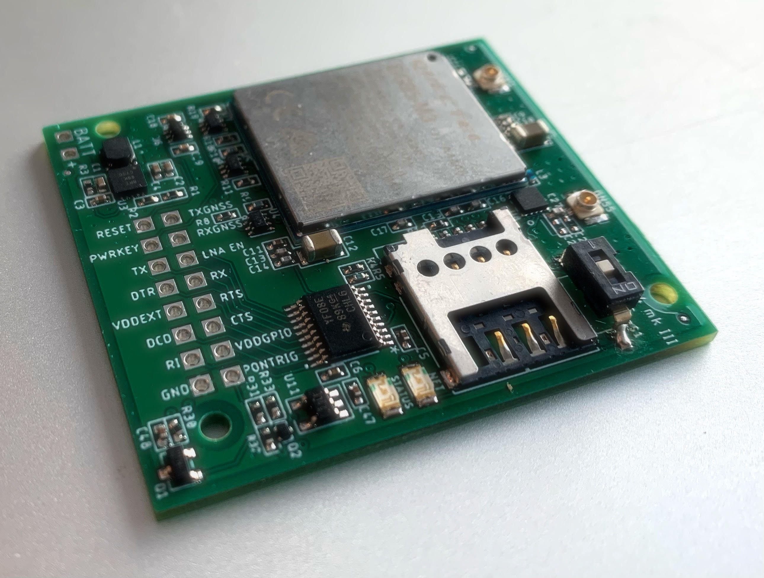
IO
The BG95-M3 has a USB interface, but I decided to not include it in the design. The only downside by not having USB being that you cannot hook the breakout up to a computer without a FTDI cable, do firmware upgrades or debug software on the BG95.
The BG95-M3 I2C interface is dedicated to communication with audio codecs. I was tempted to expose this, since it would allow the construction of a VoLTE phone based on this board, but I decided against it, since I primarilly aim to use this breakout in IoT projects and not as part of a cell phone. In addition to this, the BG95 insists on being a bus master. This means that the I2C interface would be of no use to an external microcontroller in other scenarios. I also wanted to have the breakout as clean and simple as possible.
That said - I do have a VoLTE phone project in the works, but I haven’t been able to make any calls with the hardware yet (Apart from a voiceless crank call from the module to a friend). I’m beginning to suspect that my current operator doesn’t support VoLTE, since I get CME errors from running one of the commands that are necessary to set up such a call.
UARTS
The main UART pins (TX/RX/DTR/CTS/RTS/DCD/RI) have been exposed on the IO header via a TXS0108 bidirectional voltage level translator. This allows communicating witht the module using GPIO voltages in the 1.65V to 5.5V range. This would cover any microcontroller I can think of.
But wait, there is more !
BG95 supports multiple UARTS. The GNSS has a dedicated one. Since the GNSS_TXD is a boot config pin, it complicates matters somewhat regarding using level translators with pull-ups. The GNSS RX/TX is therefore exposed on the IO header via MUN5233 pre-biased transistor arrays (This reduced the component count significantly compared to the reference design).
The jury is still out regarding the need for exposing the GNSS UART, though. Before I started digging into the AT command manual and the rather well hidden “BG95&BG77&BG600L Series GNSS Application Note” document (It seems that the easiest way to locate this document is to accidentally stumble across it on the internet, while you’re searching for something else), I was operating under the assumption that the only way to get location information out of the module was to parse NMEA sentences that was streamed from this second UART. This turns out to be incorrect. It is entirely possible to get location information and also specific NMEA sentences via the main UART using AT commands.
I may decide to not expose the dedicated GNSS uart in future revisions of this board, since it will allow me to strip 6 components and two IO pads from the board (and thereby reducing the size of the PCB).
Status LEDS
Adding LEDs to low power designs is usually a really bad idea, since they usually transform the device to a not-so-low-power-device.
Still, I decided to add two of them, since they will make the first few (usually infuriating) minutes of testing new hardware more bearable. In order to compensate for the seemingly bad design choice, I also added a way to disable them. The BG95 firmware only allows you to configure “flicker mode” or “high level output mode”. It does not provide an “off” mode. I will have to fire up the Qoitech Otii Arc and do some power profiling in order to find out how much additional power they use. Maybe the flicker mode is power efficient enough to justify having onboard LEDs.
The first LED is connected to the BG95 STATUS signal. This will light up when the module is powered on. The other one is connected to the NET_STATUS signal. This lights up when the module successfully has connected to the network.
SIM
A SIM card holder takes up more space than a SIM chip, but it enables the user to switch operators. The SIM card holder selected for this board accepts micro sized SIM cards, but I may decide to change this to nano SIM cards in a future version (In order to make the PCB even smaller).
RF & Impedance matching
The signal paths from the ANT_MAIN and the ANT_GNSS pads to their respective u.fl connectors actually kept me awake at night. I did some initial exercises with the conductor impedance calculator in the Saturn PCB toolkit, but I decided to follow the Leeroy Jenkins approach instead.
with the following a few exceptions, that is:
- I kept these RF traces as short as possible. The traces between RF pads and antennas are also 0402 pad width.
- I added a PI network to each antenna path. Such a network will allow you to tune anything to a 50 ohm impedance by using a VNA and a bit of clever Smith chart navigation.
- I added ground vias “all over the place” (though not too close to the antenna traces).
I decided to go through the tuning exercise, since it gave me an excellent excuse to get a Nano VNA V2 and learn how to use Smith charts as a tool for selecting component values for the PI networks. I found the Iowa Hills Smith Chart application quite useful for selecting the necessary values for the passive components when experimenting with antenna tuning.
I can now get away with saying stuff like “impedance matching” and “calibration plane” by the coffee machine at work :)
That said, apart from following the general layout guidelines I haven’t performed any serious tuning of the PI netowrks in the antenna paths except for verifying that I could move the impedance as close as possible to 50 ohms on an early test PCB. Both LTE and GNSS performs beyond expectation with default zero ohm resistors connecting antenna and pad.
GNSS
The BG95 has a GNSS engine that supports GPS in combination with either BeiDou, Galileo, GLONASS or QZSS. Only two constellations can be active at a given time and GPS has to be one of them.
Integrating GNSS requires a bit of additional thought. These satellites orbit at an altitude of approx 20,000km. The signal strength at ground level is extremely weak. In addition to this, your antenna is located next to another (LTE) antenna and electronics like microcontrollers and high frequency switching regulators that potentially can introduce significant amounts of electrical noise.
Enter the LNA
A LNA is a low noise amplifier that is designed to boost and in some cases also filter an incoming signal.
The reference design suggests using a Qualcomm RF360 saw filter in combination with an AR8125 LNA, The AR8125 turned out to be pretty hard to source on short notice (i.e. it wasn’t available from the usual suspects, like DigiKey and Mouser) and the design also called for 7 additional passive components along with reserving board space for 6 non-mounted passives.
I decided to try out the SKY65943 LNA from Skyworks instead. This is a GNSS RF frontend with an integrated filter that only requires one additional passive component.
(I later received engineering samples of the AR8125 from the Norwegian distributor, but this LNA didn’t make it into the design this time. Maybe later :))
The SKY65943 turned out to perform quite well. Using a passive GNSS antenna from Molex, the GNSS acquired 12 satellites on the first attempt - through my living room window.
Hello (Telco) World
We now know that the GNSS part of the board works as expected. Next up we’ll have to verify that we can communicate with something else across an LTE network.
(Spoiler alert: This blog post may end quite abruptly after we have been issued an IP address, since this will demonstrate that the module successfully has connected to a network, and that obscure in-between stuff like RADIUS access requests have been accepted and that there is light at the end of at least one ipsec tunnel. I will follow up with another blog post that describes how to interface the module to a microntroller board and how to transmit sensor data with it)
I have used a 3.7V Li-Ion battery for these tests, but the breakout should be able to run on anything from 1.8V to 5.5V (Keeping in mind that more current can be provided in step down mode than in step up mode. Tests will have to be performed in order to determine the minimum acceptable voltage :)). 3 x AA batteries or a benchtop power should also work nicely. Since there is no polarity protection on the BATT connectore, we’ll just have to observe polarity and also make that we don’t exceed 5.5V.
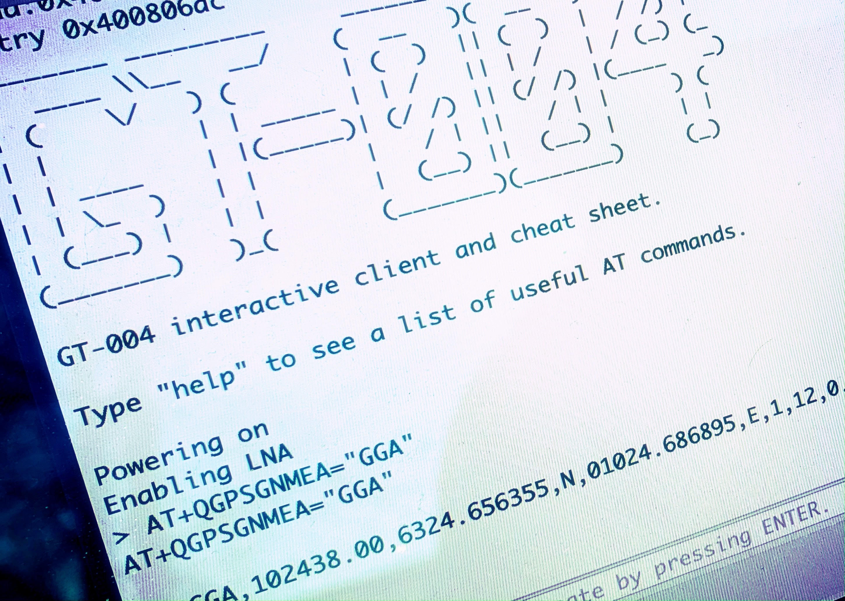
First we have to check that the board powers on.
After applying power, nothing much will happen. Until we…
pull the PWRKEY ping high for half a second. This will wake the module and the STATUS LED will turn on. The module is now running and commands can be sent via the UART. Hardware flow control is not enabled by default and using only the TX/RX lines is sufficient.
The command line termination character defaults to <CR> (ASCII 13). If desired, this can later be changed by using the “ATS3=<n>” command (where <n> is the new termination character).
The default UART configuration is 115200 8N1. Cross the TX/RX lines when connecting to a microcontroller or FTDI cable and you’re ready to go.
The first test is to send the following command.
AT
This does absolutely nothing, except to force the module to respond with “OK”. This tells us that we can proceed with the necessary AT commands that will configure the module correctly for our scnario, which is LTE-M.
The next task is to query the status of the SIM card.
AT+CPIN?
If the module responds with “+CPIN: READY”, we’re good to go, but if it responds with “+CPIN: SIM PIN”, we will have to unlock the sim by sending
AT+CPIN=“<pin>"
before we can proceed.
We will need two unique identifiers in order to register the module with our backend server.
These are:
- IMEI (International Mobile Equipment Identity). We acquire this by sending the following command:
AT+GSN
- IMSI (International mobile subscriber identity). This is acquired by sending the following command to the module:
AT+CIMI
Since we are software people, we will of course use our own Span backend. If you’re curious, about it, I suggest you take a look at the management console. This can be accessed from https://span.lab5e.com/. (I guess Span is deserving of a whole series of blog posts, so I will not go into details regarding the backend server here).
Since this version of the board has a rather wimpish power supply, we’ll steer clear of 2G and configure the module to scan for LTE only. We do this by sending the following command:
AT+QCFG="nwscanmode",3,1
Similarly, we might want to select which network categories to be searched (eMTC/LTE Cat M1 or NB-IoT). Chapter 4.2.3 in the “BG95&BG77 AT Commands Manual” describes how to use iotopmode.
With RAT and IoT technologies selected, we can move on to PDP (Packed Datagram Protocol) context.
AT+CGDCONT=1,"IP","mda.lab5e"
The first argument in this command is the context identifier. We’ll refer to this in the next command. The second argument specifies that we are going to use IPv4. The third argument is the name of our APN. By using the mda.lab5e APN. Data that you send will magically appear in the Span backend (if you have a NB-IoT or LTE-M enabled Telenor SIM card, that is :)).
The next command will activate the PDP context. The first argument is the state (0: deactivate, 1: activate), and the second argument is the PDP context id that we specified when defining the context.
AT+CGACT=1,1
Magic should start happening on the air after we have executed this last command.
We can run the
AT+CEREG?
command if we want to query the LTE network registration status. We’re interested in the last number in the response from this command. If this is “1” we’re registered on the home network, “0” or “2” means that it is still searching for an operator to connect to or trying to attach. “5” means that the module is registered, but roaming. “3” is denied and “4” probably a polite way of indicating that you have done something wrong along the way.
Anyway, “registered” is good. Anything else requires more coffee or maybe a quick read through of the 201 page AT commands manual.
The next step is to see if our backend has issued us with an IP address by running
AT+CGPADDR
, or maybe we’ll just take a look at the management console in Span…
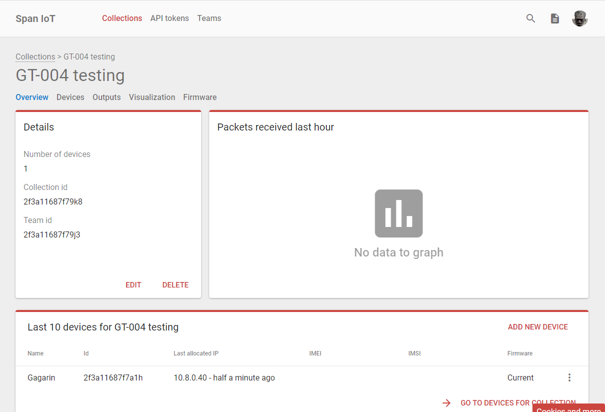
Mission accomplished. We have an IP address. We are online :)
(I took the liberty of removing the IMEI and IMSI numbers from this screen dump :))
Future work
Changes considered for future iterations
- Nano SIM card.
- Fewer exposed GPIO pins
- Beefier power / Diode ORing of solderable regulators.
- Enable line for main power
- Shields for Arduino, ESP32, Raspberry Pi.
References
The following reference manuals are available from the Quectel download center:
- “BG95 Hardware Design”
- “BG95&BG77 AT Commands Manual”